The Atomic Force Microscope (AFM) is one of the foremost tools for imaging, measuring, and manipulating matter at the nanoscale. The information is gathered by running a mechanical probe across the surface. Piezoelectric elements that facilitate very small but accurate and precise movements on command enable the very precise scanning.
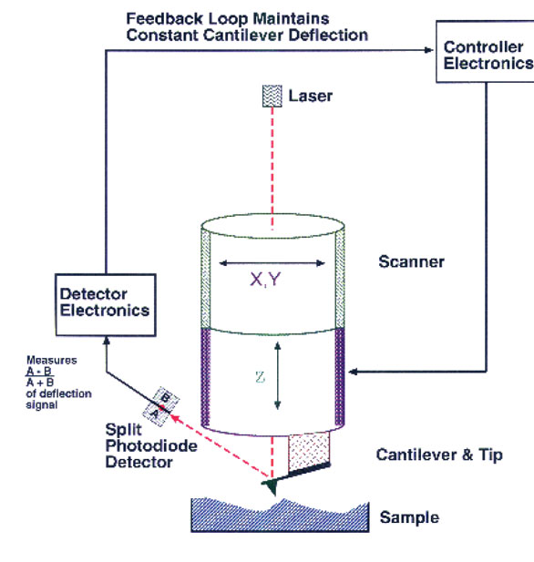
The AFM consists of a cantilever with a sharp tip (probe) at its end that is used to scan the specimen surface. The cantilever is typically silicon or silicon nitride with a tip radius of curvature on the order of nanometers. When the tip is lowered into the proximity of a sample surface, forces between the tip and the sample lead to a deflection of the cantilever. Typically, the deflection is measured using a laser which focused, then reflected, from the top surface of the cantilever into an array of photodiodes.
Unlike the electron microscope which provides a two-dimensional projection or a two-dimensional image of a sample, the AFM provides a true-three-dimensional surface profile. Additionally, samples viewed by AFM do not require any special treatments (such as metal/carbon coatings) that would irreversibly change or damage the sample. Also, while an electron microscope needs an expensive vacuum environment for proper operation, most AFM modes can work perfectly well in ambient air or even a liquid environment. This makes it possible to study biological macromolecules and even living organisms. In principle, AFM can provide higher resolution than SEM. The AFM has the advantage of imaging almost any type of surface, including polymers, ceramics, composites, glass, and biological samples. More importantly, chemical and mechanical material properties including surface adhesion, hardness, and friction may be measured. AFM tip can be chemically modified in order to measure tip/sample interactions. In some variations, electric potentials can also be scanned using conducting cantilevers. With good samples, meaning they are clean with no excessively large surface features, resolution in the x-y plane ranges from 0.1 to 1.0 nm and in the z-direction is .01 nm.
Some disadvantages include scanning speed, sample space, and potential surface damage. Samples may take several minutes at a time in order to create an image, unlike the SEM which can create an image in almost real time. Also, AFM can only image a maximum height on the order of 10-20 micrometers and a maximum scanning area of about 150 X 150 micrometers. AFM, particularly in Tapping Mode, is non destructive. Tip forces are finely controlled, but in Contact Mode the surface of samples may be damaged or the sample may even be pushed out of the control area. Besides these minute inconveniences, Atomic Force Microscopy is a powerful tool allowing a variety of surfaces to be imaged and characterized at the atomic level. It has been shown to give true atomic resolution in ultra-high vacuum (UHV) and, more recently, in liquid environments.